Samsung's new 3nm process promises better performance in a smaller footprint
The company has kicked off initial production of 3nm chips.

What you need to know
- Samsung has begun production of its advanced 3nm-based chips.
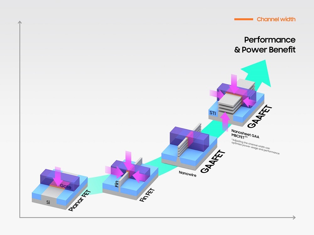
- The process uses the gate-all-around (GAA) architecture to improve performance while reducing power usage.
- Samsung beats TSMC to advanced chip fabrication process.
Samsung has kicked off initial production of its 3nm process node, which uses the gate-all-around (GAA) transistor architecture to boost performance while reducing power usage.
The new process promises improved performance in a smaller surface area than the 5nm process. Samsung claims the first-generation 3nm process cuts power usage by 45%, while improving performance by 23% and shrinking the surface area by 16% compared to 5nm. The second generation promises even better performance: 50% less power consumption, 30% improved performance, and 35% smaller surface area.
Bloomberg reports that the South Korean tech giant will begin mass production of next-generation chips in the first half of 2022. According to the report, Samsung is the first to begin producing 3nm chips, beating TSMC to the punch.
Samsung notes that the use of Multi-Bridge-Channel FET marks the first time the GAA technology is put into use.
Samsung says it's using semiconductor chips to start the first application of the nanosheet transistor before extending it to mobile processors, which will power tomorrow's best Android phones. These types of chips are designed for high-performance and low-power computing applications.
The company uses the 3nm GAA technology to adjust the channel width of the nanosheet: the wider a nanosheet's channel, the higher performance and greater energy efficiency it achieves. This is in contrast to existing GAA technologies that use nanowires with narrower channels.

This technique is designed to optimize power in order to meet various practical needs of customers. Samsung is producing 3nm chips at its Hwaseong-based facilities, with plans to expand the work to its Pyeongtaek fab, as per Bloomberg.
Be an expert in 5 minutes
Get the latest news from Android Central, your trusted companion in the world of Android
The initial production begins following reports in April that Samsung was having trouble with its new GAA 3nm manufacturing process due to low yield rates.
The company appears to have addressed those issues, though it still needs to perfect its 3nm chips in order to outperform Qualcomm's Snapdragon line. The next processor from the semiconductor giant is likely to be built on a 3nm process as well. It will presumably be known as Snapdragon 8 Gen 2.

Jay Bonggolto always keeps a nose for news. He has been writing about consumer tech and apps for as long as he can remember, and he has used a variety of Android phones since falling in love with Jelly Bean. Send him a direct message via Twitter or LinkedIn.
